Identify layer thickness distribution over boards and panels
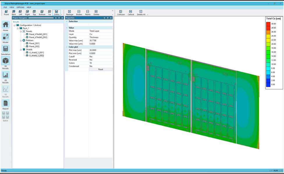
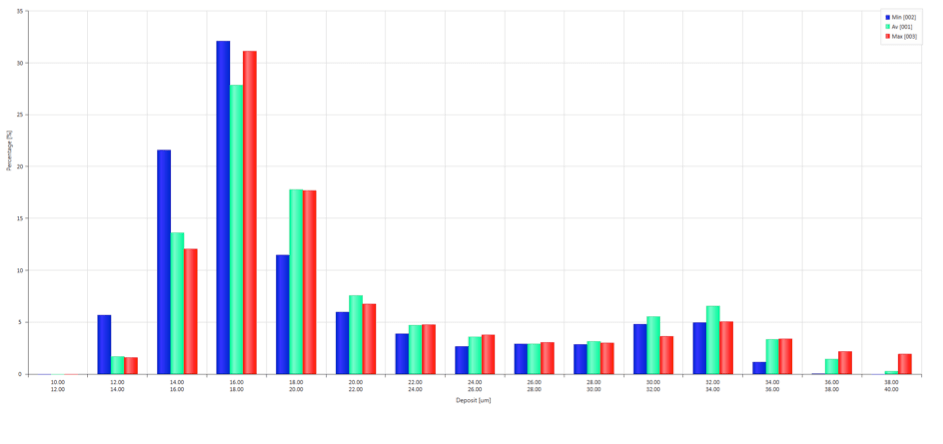
Generate color plots of layer thickness distribution and related production risk zones over the boards and panels. Produce 2D bar charts for efficient production variance analysis.
Generate color plots of layer thickness distribution and related production risk zones over the boards and panels. Produce 2D bar charts for efficient production variance analysis.
Your real-life panel and pattern plating tanks, including their particular plating chemistry, are pre- configured by Elsyca in your installed version of the Elsyca PCB software, no need for spending time and effort on this.
Understand the impact of your board design and panel layout on the layer thickness distribution with just a few clicks.
Generate detailed information on the layer thickness inside holes.
Easy incorporation of PCB layout information: ask your colleagues from the CAM department to export the PCB layout in Extended Gerber format (available in almost every CAM package) and import directly into the Elsyca PCBPlate database.
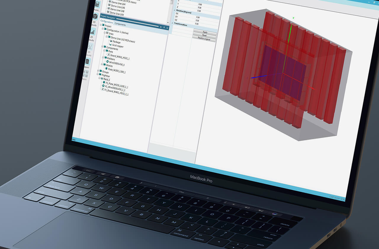
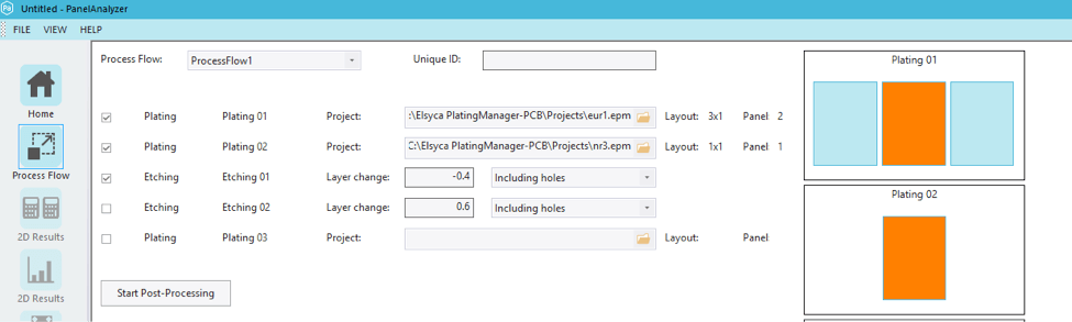
Panel Analyzer computes total layer thickness distribution over the panel/holes for one panel, while accounting for the full panel history: position of the panel on the flight bar and process parameters for each plating step, as well as other relevant steps like etching or electroless deposition
The consistency of the plating package is verified upfront
Robust and fast simulation of the current density and layer thickness distribution over all panels
Easy what-if simulation to verify the impact of layout modifications, tooling (shielding, current robbers, or even auxiliary anodes), different panel configurations and loads (and thus production capacity) and process parameter modifications.
Elsyca PCBPlate supports the free standalone Elsyca XPlorer viewer, the visualization and post-processing environment that allows sharing color plot results with other stakeholders.
Automated yet customizable reports are generated at the end of the simulation process, in support of ISO quality processes
Visualize the risk zones (out-of-spec layer thickness) on the panel and adapt the board design, panel layout, process parameters or tooling design accordingly.
Production optimization can be done before the panels are manufactured. Avoid lengthy trial-and-error runs and stressful production surprises. Buy yourself some peace of mind.
Avoid trial runs and reduce plating problems without the necessity for increasing plating times, ... it all leads to higher profits for your company.
Elsyca PCBPlate is an investment in knowledge as it helps to accumulate and store critical company know-how.
Become a value-adding partner for your customer. Advice your customer on DFM using comprehensive simulation results, Build up knowledge by using intelligent simulation software and enhance your overall service level.
You can use the software for DFM purposes, based on a virtual plating line. Simulations can also be executed using a virtual mock-up of your in-house PCB plating tanks, and provide detailed information on copper layer thickness distribution and potential quality issues over the different panels on the flight bar.
Alternative panel configurations can be investigated in only a few mouse clicks. Moreover, additional tooling components like shields or robbers can be introduced and their impact quickly verified. For enabling the simulation of pattern electroplating processes, the top and bottom layout of the PCB job under investigation are obtained from Extended Gerber file input data.
Ingenious in its simplicity, no CAD or CAM skills required. As a user, just define the panel size, load the Gerber layout file, set the process parameters, and press the simulation button. It is really that simple!


Elsyca PCBPlate is a state-of-the-art PCB plating simulation platform providing detailed layer thickness distribution information over the panels, patterns and inside holes.
To ensure the simulation results provide accurate and reliable information, a validation study was executed on panels produced by Eurocircuits (www.eurocircuits.com). The setup was a combination of different boards on a panel, in a 2x2 panel layout.
Fig1: panel layout flightbar
Different measurement points were defined on the front/back side of the panels as well as areas of interest for through-holes.
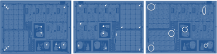
Fig 2: location measurement points front side/back side and area holes front side
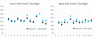
The layer thickness distribution was computed for all panels, what follows are the simulation and measurement results of the panel at the upper right position on the flight bar.
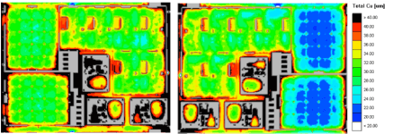
Fig 3: front side on the left, back side on the right
The maximum/minimum layer thickness values where measured inside the holes in the selected areas, and compared with the simulation results. The results are shown in the graph below.
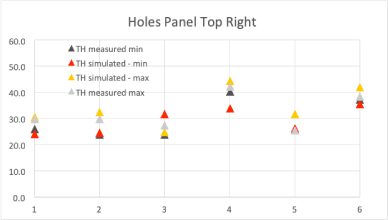
Summarizing the measured/simulated maximum/minimum values in the holes:
Minimum value | Maximum value | |
Average measured thickness | 29.5 | 32.4 |
Average simulated thickness | 29.4 | 34.4 |
Deviation | -0.4% | 5.9% |
Next, the values at the pre-defined measurement points were compared:
Summarizing the measured/simulated values on the panel/pattern:
Front side | Back side | |
Average measured thickness | 33.6 | 29.8 |
Average simulated thickness | 36.1 | 32 |
Deviation | 7.4% | 7.2% |
The validation study proves the software provides a +90% accuracy level for the simulated layer thickness value.This implies the Elsyca PCBPlate users can rely on the simulation results to upfront validate different design, panel layout or process configurations.
Elsyca NV
Vaartdijk 3/603
B-3018 Wijgmaal (Leuven)
Belgium
Phone: +32 16 474960
info@elsyca.com
www.elsyca.com
Or drop us a line